Assemble the EIB
See section on custom parts for details on how to design and order the printed circuit boards (PCBs) for the EIB. If a commercial EIB provided by the maker of your electrophysiology system is used, just clean the EIB with ethanol.
Clean the PCB with ethanol.
Solder the headstage connector to the pads on the EIB:
You'll need: the EIB, a flux pen (like this one at amazon), a soldering iron with a thin and long tip, and the omnetics connectors.
First, 'tin' (apply solder) to the pads on the eib. The aim is to get enough solder on there so that you don't need to add any more when soldering the connector. The right amount should look like little domed or pillow-like bumps on each pad. If adjacent pads are connected with solder, it might cause problems later. To tin the pads, hold the eib in a clamp, apply some flux to the pads, and swipe them with a soldering iron with solder on it. Avoid the vias, once you accidentally get solder in them it's a bit hard to remove (if it happens, use a desoldering gun or braid with plenty of flux).
If you applied too much solder, either move it away with the soldering iron, or use some solder wick.
(add picture here)
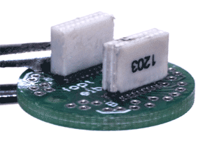
Now that each pad has a little bump of solder on it, apply more flux and place the connector on the pads and hold it there (holding it with one finger while the eib is clamped works pretty well). Make sure that the 'feet' of the connector are centered on the pads - they'll want to slip off the solder bumps so this part is a bit tricky.
If you applied too much solder, either move it away with the soldering iron, or use some solder wick.
(add picture here)
Now that each pad has a little bump of solder on it, apply more flux and place the connector on the pads and hold it there (holding it with one finger while the eib is clamped works pretty well). Make sure that the 'feet' of the connector are centered on the pads - they'll want to slip off the solder bumps so this part is a bit tricky.
If you're happy with the placement, carefully tap the feel of the connector from above, one at a time. Start with two corners to secure the part, then go through the others. Each time, you should feel that after a very short time, the contact gives in a bit as the solder melts and the contact is pushed down a bit.
Once one side is soldered, repeat the same procedure on the other side. On boards with two connectors, the 2nd connector will be a bit harder to work with because the medial side will be obscured by the 1st connector. Use a long tip on your iron, and try to avoid melting the top of the omnetics connectors by coming in from the sides rather than from the top. Melting the sides of the connectors a bit is not pretty but shouldn't interfere with function.
Alternatively, the connectors can be soldered to the EIB by using soldering paste and an ordinary toaster oven. This makes most of the above steps unnecessary. We have got excellent results by following the instructions on this link:
The most important advice is to use very little soldering paste. To figure out the right amount, it is better to run a few tests on disposable electric circuits.
Next, clean the flux off the PCB (unnecessary if you used a toaster oven).
Test the connections and check for shorts between traces.
If the PCB design has separate circuits for reference and ground channels, these can optionally be joined either by soldering a short piece of stainless steel wire between the corresponding vias, or by placing a solder bead to short the corresponding SMD pads.
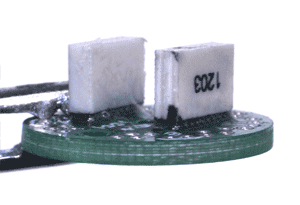
Reinforce the joint of the connector to the EIB with epoxy. Without this step, the solder connection can break after a few connect/disconnect cycles. Be careful to avoid getting any epoxy into the vias, as small amounts can be very hard to spot and can cause connection problems when loading electrodes later.
(optional) connect GND to REF or connect two REFs and GNDs
On many EIBs, there is a built-in way to tie REF and GND together with either a solder bead or by briding two vias with a small piece of wire. In some cases, they might be tied together by default and a trace needs to be cut to separate them if desired.
On EIBs with two connectors that have independent GND and REF connections, it might make sense to connect these together by feeding one wire through ground&ref (or separate GND and REF depending on application) wire through the appropriate vias and soldering it. This results in two free ends to the wire, one for the shield, the other for the GND screw with minimal soldering etc.
The EIB is now ready to be glued onto the drive body.