PCIe prototype
- Jakob Voigts
lets use this page to archive some key information on the development of the prototype PCIe board.
The main github repo for this is (for now - we might move this later): https://github.com/open-ephys/next-gen-system
The interface specifications etc are on: PCIe acquisition board (Open Instruments) standard
Also see out slack channel at https://open-ephys.slack.com (email us to get an invite)
Progress (May6)
- Jon and Jakob, and goncalo/adam have dev boards, one on route to aaron, (will have one spare) done
- Started to design simple FMC card for testing intan chips (github) done (MIT)
- verify basic building blocks of FMC hardware design (MIT & UCL) done
- decide on which DMA architecture to use - try xilybus for now, seems fastest way to working prototype done
- verify basic DMA firmware function and xilinx vivado version control done
- implement simplest working design for streaming intan data via DMA done (Aaron)
- implement simple output registers done (Aaron)
- Measure throughput round-trip latency to software buffer: done (Jon, Jakob)
Read stream of data from FPGA to GUI app, send pulse to an FPGA pin, detect this in software and trigger an output pin on the FPGA, measure latencies.
See below and blog post - Try latencies etc in Bonsai
Hardware
We're using a kintex 7 eval board (http://www.xilinx.com/products/boards-and-kits/kcu105.html)
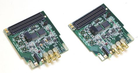
with a custom FMC daughter card (https://github.com/open-ephys/next-gen-system/tree/master/FMC-board)
that provides
- 3x direct SMA connectors to the fpga, with overvoltage diode protection.
- 2x intan compatible 12pin omnetics connectors (A & B) for the intan headstage SPI standard, wired directly to the fpga, with a power supply.
- 1x isolated intan compatible connector (C) isolated through LVDS to CMOS converters and galvanic isolators. This headstage has its own power supply that is fed through am isolated DC-DC converter.
- 3x directional SMA connectors (on the card front edge) that are routed through the same isolation circuit as headstage connector C
For testing we should aim to use the isolated pins, but we added non-isolated ones in case there's an issue with the isolation circuitry.
The FPGA <> FMC pinout is at https://docs.google.com/spreadsheets/d/18WfmbLGt8bGUUdksKp6AKA_wMX2SJ3Tndin-nnEgUCs/edit#gid=584734392
Test setup: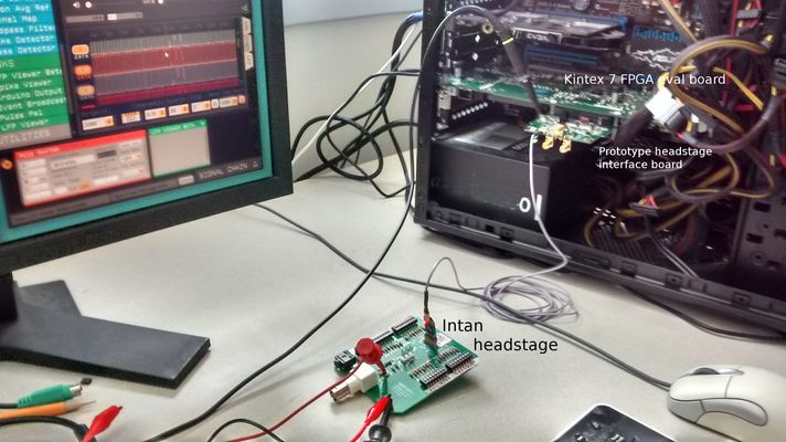
DMA interface
The main issue here is how to implement the intan <> GUI transfer via DMA.
Xillybus see here for specifications
Pro: Seems very easy to implement
Cons: closed, licensing likely not compatible with wide adoption
Performance measurements
Measuring round-trip latencies from the open ephys GUI is problematic because of the latencies caused by the processing chain callback and buffer overheads.
For submillisecond feedback it makes more sense to just call the feedback function directly from the data acquisition thread, or in a separate thread that receives data directly from the DMA interface but is not subject to the timing and buffering requirement of the whole processing pipeline.
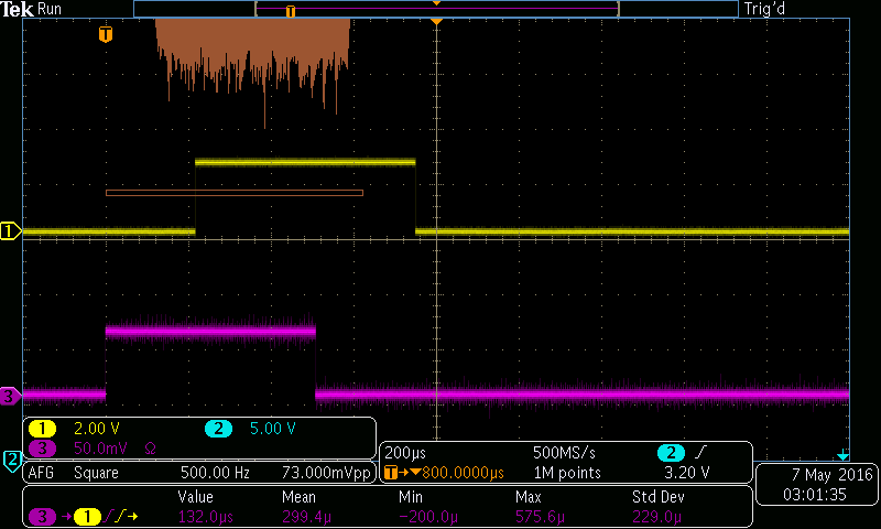
For testing, Aaron patched a simple threshold detector into the PCIe interface plugin in the Open Ephys GUI, to send a response output whenever the input voltage at the headstage is over a threshold. We ran these tests on a stock 16.04 Ubuntu system with an Intel core i7-3770K @ 3.5GHz.
For input buffer sizes (via Xillybus DMA interface) of 1 sample (33us) we get this:
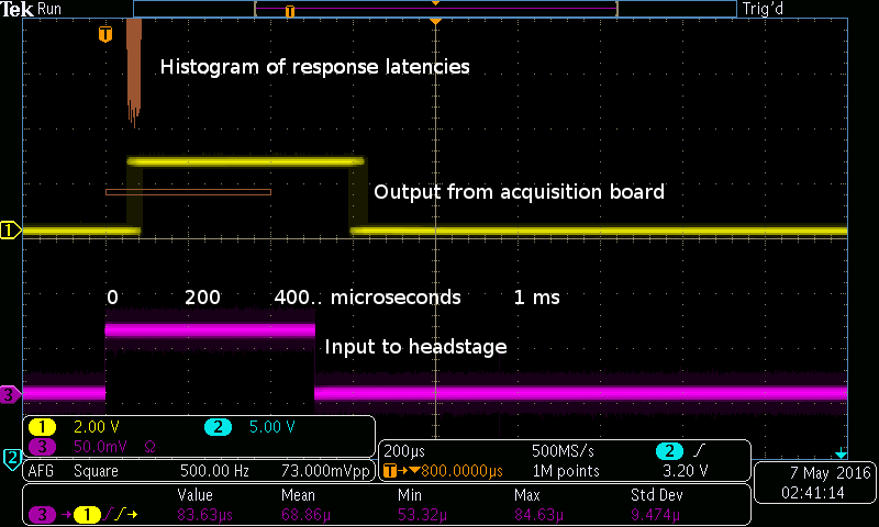
When increasing the input buffer sizes, the min. latencies go up a bit, and an extra jitter of ~33us/sample (30kHz) is added:
it looks like none of this is necessary in practice though because the system should be able to handle required channel numbers even at this somewhat wasteful 1 sample buffer size.
2 samples/buffer: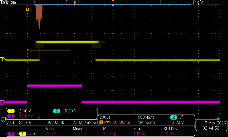
16 samples/buffer (the min/mean/max are invalid here, the histogram is correct):