Creating graphics of PCBs for documentation
- Josh Siegle
- Alex Leighton
This page provides a step-by-step guide to creating beautiful graphics that can be used to publicize and document your hardware designs.
Prerequisites
This tutorial assumes you're starting with a printed circuit board design in Eagle, and that you have access to Adobe Illustrator.
Step 1: Obtain the Eagle .brd file
You can either follow along with your own .brd file, or use the one provided. This tutorial will be based on the open-source design file for Intan's 16-channel headstage based on the RHD2132 chip: RHD2132_headstage_16.brd
Step 2: Export a .dxf
NOTE: If you want to skip this step, you can download RHD2132_headstage_16.dxf
Open the .brd file in Eagle. Click the "Ratsnest" ![]() button to ensure all ground and power planes are filled in. Then select the "Display"
button to ensure all ground and power planes are filled in. Then select the "Display" ![]() button to select which layers to show. Eagle's .dxf creator will only export visible layers. For the purposes of this tutorial, you should hit the "None" button, then make sure "Top," "Pads," "Vias," "Dimension," "tPlace," and "tNames" are selected.
button to select which layers to show. Eagle's .dxf creator will only export visible layers. For the purposes of this tutorial, you should hit the "None" button, then make sure "Top," "Pads," "Vias," "Dimension," "tPlace," and "tNames" are selected.
Finally, click the "User language program" ![]() button and select "dxf.ulp". Check that the default settings look fine, and click "OK."
button and select "dxf.ulp". Check that the default settings look fine, and click "OK."
Step 3: Process the various layers in Illustrator
- Outline
- Ensure only the bottom layer (20) is visible
- Select all (cmd/ctrl-A) and Join (cmd/ctrl-J)
- Change the Stroke to black, 0.25; change the Fill to a nice vertical gradient
It should look something like this:

- Pads
- Lock the outline layer and make the "top" layer visible (1)
- Select one of the pads (not the traces) and then choose "Select > Same > Fill Color"
- Join the filled areas with the "Pathfinders > Merge" utility
- Change the fill color to light gray (or deep yellow to represent gold immersion plating)
- Copy the pads, create a new layer, and choose "Edit > Paste in place" (shift+cmd/ctrl-V)
- Delete the pads from the previous layer
It should now look something like this:
- Traces
- Hide the pads layer and go back to the "top" layer (1)
- Choose "Select > Same > Stroke Color"
- Choose "Object > Expand", make sure "Fill" and "Stroke" are selected, and click "OK"
- Join the traces with the "Pathfinders > Merge" utility
- Change the fill color to something slightly darker than the background (in this case, black)
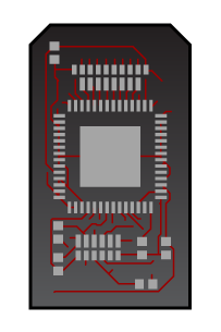
It should now look like this:
Holes
- Lock the visible layers, and make the Holes (17) and Vias (18) layers visible
- Select all (cmd/ctrl-A)
- Set the stroke size to 0.25 mm, the Fill to white, and the Stroke to light gray
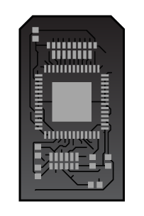
You should now have something like this:
- Silkscreen
- Lock the visible layers, and expose the two remaining layers (21 and 25)
- Delete any lines that overhang the edge of the outline (in this example, just those at the bottom of the board)
- Select all (cmd/ctrl-A)
- Choose "Object > Expand", make sure "Fill" and "Stroke" are selected, and click "OK"
- Join the traces with the "Pathfinders > Merge" utility
- Change the fill color to white, and the transparency to 80%
- Delete the empty layer (21), and make sure the silkscreen layer is above the traces, but below the pads and vias
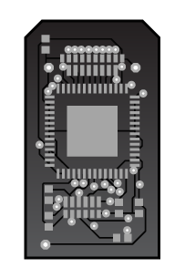
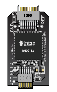
Here's the final PCB design:
Step 4: Add surface-mount and through-hole components
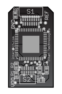
This step is more subjective, and may require some amount of artistic license. Create a new layer called "Components" above the other layers, and draw your components there. If you want to copy components from an existing Illustrator file, you can use the ones in the final document: RHD2132_headstage_16.ai
This is what the board will look like once it's "populated":
Step 5: Export for the web
We like to us the "File > Export" function to generate high-quality PNGs (300 dpi or higher). Using artboards will help you keep the size of your images consistent, no matter which layers are visible.